Join World's Fastest Growing B2B Network
Join World's Fastest Growing B2B Network


| Quantity | 1 - 9 | 10 - 99 | 100+ - 100+ |
| Price | US $7.50 | US $7.40 | US $7.20 |
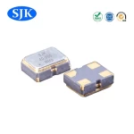
| Model NO. | TG5032SFN | Operation Temp / Humidity | -40 to 85u00baC |
| Product Name | Crystal Oscillator | Dimensions (W X D X H) | 5.00mm X 3.20mm |
| Output | 3.3V | Net /Gross Weight | Customized |
| Transport Package | Carton Packing | Trademark | EPSON |
| Origin | China |


|
Item Symbol TG5032CFN (CMOS output)
TG5032SFN(Clipped sine wave) Conditions /
Remarks TCXO VC-TCXO TCXO VC-TCXO Output
frequency
range fo 10 MHz to 40 MHz 10, 12.8, 19.2, 20, 24.576, 25, 25.6, 26, 30.72, 38.4, 38.88, 40 MHz Standard frequency Supply voltage VCC C: 3.3 V ± 5 % (Supply voltage range: 2.375 V to 3.63 V) Storage temperature T_stg -40 ºC to +90 ºC Storage as single product Operating temperature T_use G: -40 ºC to +85 ºC Standard temp. range a) Frequency tolerance f_tol ±1.0 × 10⁻⁶ Max. After reflow, +25 ºC b) Frequency/temperature Characteristics fo-Tc A: ±0.1 × 10⁻⁶ Max. / -40 ºC to +85 ºC H: ±0.25 × 10⁻⁶ Max. / -40 ºC to +85 ºC B: ±0.28 × 10⁻⁶ Max. / -40 ºC to +85 ºC Reference to (fmax + fmin) / 2 c) Frequency/load coefficient fo-Load ±0.1 × 10⁻⁶ Max. Load ± 10 % d) Frequency/voltage coefficient fo-VCC ±0.1 × 10⁻⁶ Max. VCC ± 5% e) Frequency aging f_age ±0.5 × 10⁻⁶ Max. +25 °C, First year ±3.0 × 10⁻⁶ Max. +25 °C, 20 years Holdover stability (Constant temperature) - ±0.01 × 10⁻⁶ Max. ( +25 °C , 24 hours) After 10 days of continuous operation. ±0.04 × 10⁻⁶ Max. ( +25 °C , 24 hours) After 48 hours of continuous operation. Wander generation (MTIE, TDEV) - - Compliant with GR-1244CORE , ITU-T G.8262 Free-run accuracy - ±4.6 × 10⁻⁶ Max. This includes Item a), b), c), d) and e) Current consumption ICC 5.0 mA Max. 5.0 mA Max. 10 MHz ≤ fo ≤ 26 MHz 6.0 mA Max. 26 MHz < fo ≤ 40 MHz Input resistance Rin - 100 kΩ Min. - 100 kΩ Min. VC- GND (DC) Frequency control range f_cont - ±5 ×10⁻⁶ to ±10 ×10-6 - ±5 ×10⁻⁶ to ±10 ×10-6 D :Vc = 1.5 V ± 1.0 V at VCC = 3.3 V E :Vc = 1.65 V ± 1.0 V at VCC = 3.3 V Frequency change polarity - - Positive polarity - Positive polarity Symmetry SYM 45 % to 55 % - 50 % VCC level, L_CMOS 15 pF Output voltage VOH 90 % VCC Min. - VOL 10 % VCC Max. - Output level Vpp - 0.8 V Min. Peak to Peak Rise time / Fall time tr/tf 8.0 ns Max. - 10 % VCC to 90 % VCC level, Load: 15 pF Start-up time t_str 5.0 ms Max. t = 0 at 90% VCC Output load condition Load 15 pF 10 kΩ // 10 pF |


One moment please
 Member's Area
 Messages
  Need Help