Join World's Fastest Growing B2B Network
Join World's Fastest Growing B2B Network


| MOQ | 5 Pieces |
| Port | Shenzhen Port |
| Packaging | As Per Costumer Request |
| Lead Time | 14-21 Days |
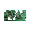
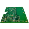
| Product Name | 1.8mm Thickness 2OZ Copper Custom PCB Boards With 6L Max Layer | Keywords | PCB, PCBA, Printed Circuit Board Assembly, Chinese Manufacturer |
| Packaging | As Per Costumer Request | Port | Shenzhen Port |
| Company Name | Bingo Electronics Technology Development | Origin | China |

Capabilities overview:
| Layers: | Rigid PCB 2 - 40 + Layers, Rigid-flex PCB 1 - 10Layers |
| Panel Size(max): | 21" x 24" |
| PCB Thickness: | 0.016" to 0.120" |
| Line & Spaces: | 0.003" / 0.003" Inner Layers; 0.004" Outer Layers |
| Hole Size: | 0.006" Thru Hole (Finished Size) and 0.004" Buried Via |
| Materials: | FR4, High Tg, Rogers, Halogen-free material, Teflon, Polyimide |
| Surface Finishes: | ENi/IAu, OSP, Lead-free HASL,Immersion Gold/Silver, Immersin Tin |
| Special Products: | Blind/ Buried Via(HDI 2+N+2), Rigid Flex |
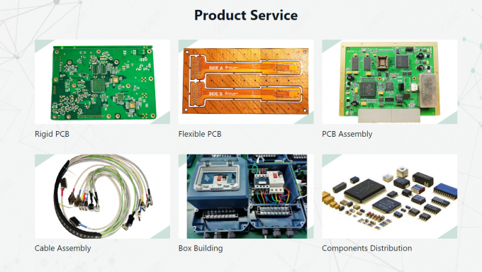
Our company provide:
FAQ:
Q1: What files do you use in PCB fabrication?
A1: Gerber, BOM,Drawings.
Q2: How do you make sure the quality?
A2: Our Product is all 100% E-tested .PCB Assembly are with 100% AOI,ICT,FT and Visual checking,100% X-ray for BGA.
Q3: Can we visit your company?
A3: Of course,Welcome to visit our company, Bingo Electronics Technology Development located in No 6 Building, Xitian Industrial Park, Shangcun Village, Guangming City, Shenzhen, Guangdong, China.
Q4: What is the lead time?
A4: It takes 3-5 working days for sample, 7-10 working days for batch production based on files and quantity. It takes 15-20 working days for PCB assembly.
Q5: Will you keep our information and files secret?
A5: Sure,It is our basic principle to keep business secrets to protect our customers' designs.NDA can be signed at any time.
Q6. How to work with you?
A6: -Email and send us the PCB layout file, BOM list
No 6 Building, Xitian Industrial Park, Shangcun Village, Guangming City, Shenzhen, Guangdong, China
One moment please
 Member's Area
 Messages
  Need Help